The Future of PCB Design: Trends and Innovations
Printed Circuit Boards (PCBs) are at the heart of almost every electronic device we use today. As technology continues to advance, the field of PCB design is also evolving rapidly. In this article, we'll explore some of the key trends and innovations shaping the future of PCB design. Read on rogers 4350b to discover more.
Miniaturization and High-Density Interconnects
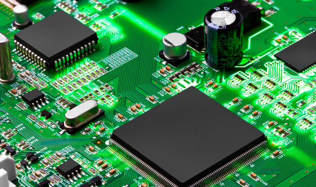
One of the most prominent trends in PCB design is the relentless drive towards miniaturization and higher component density. As consumers demand smaller and more powerful devices, PCB designers are challenged to accommodate more functionality within limited space. High-Density Interconnect (HDI) technology allows for finer traces, smaller vias, and more layers, enabling the creation of compact yet highly functional PCBs.
3D PCB Design
Traditional PCBs are flat, two-dimensional structures. However, 3D PCB design is gaining traction, allowing designers to create PCBs with three-dimensional shapes and features. This innovation is particularly valuable in applications where space is constrained or where PCBs need to fit into irregularly shaped enclosures. 3D design also facilitates more efficient cooling and heat dissipation.
Advanced Materials
The choice of materials in PCB design is expanding to meet the demands of high-frequency and high-speed applications. Materials like specialized laminates and ceramics offer superior electrical performance and thermal management capabilities. These materials enable PCBs to operate at higher frequencies and handle more data, making them essential for applications like 5G communication and high-speed data processing.
Flexible and Rigid-Flex PCBs
Flexible PCBs (FPCBs) and rigid-flex PCBs are becoming increasingly popular for applications where flexibility and durability are essential. These PCBs are made from flexible materials like polyimide and can be bent or twisted to fit specific form factors. They are commonly used in wearables, medical devices, and aerospace applications where traditional rigid PCBs would be impractical.
Internet of Things (IoT) Integration
The Internet of Things (IoT) is driving innovation in PCB design. IoT devices often require low power consumption, small footprints, and wireless connectivity. PCB designers are working to create specialized PCBs optimized for IoT applications, allowing for seamless integration of sensors, communication modules, and power management components.
Design for Manufacturability (DFM)
Design for Manufacturability (DFM) is a growing trend in PCB design. It involves considering manufacturing processes, cost-effectiveness, and ease of assembly from the very beginning of the design process. DFM practices aim to reduce errors, lower manufacturing costs, and ensure that the final PCB design is optimized for efficient production.
Artificial Intelligence (AI) and Automation
Artificial intelligence and automation are transforming the PCB design process. AI algorithms can analyze complex design requirements and suggest optimal layouts, component placements, and routing paths. Automation tools streamline repetitive tasks, increasing productivity and reducing design time. These technologies empower designers to focus on creativity and innovation rather than manual labor.
Sustainability and Green Design
With a growing emphasis on environmental responsibility, there is a push towards sustainable and eco-friendly PCB design. This includes using recyclable materials, reducing waste, and minimizing the use of hazardous substances. Compliance with regulations like RoHS (Restriction of Hazardous Substances) is becoming standard in the industry.
Conclusion
The future of PCB design is marked by continuous innovation to meet the demands of smaller, more powerful, and environmentally conscious electronic devices. From miniaturization to 3D design, advanced materials, flexible PCBs, IoT integration, DFM, AI, and sustainability, the PCB design landscape is evolving to support the ever-expanding world of electronics. As technology continues to advance, PCB designers will play a pivotal role in shaping the future of electronic devices and systems.